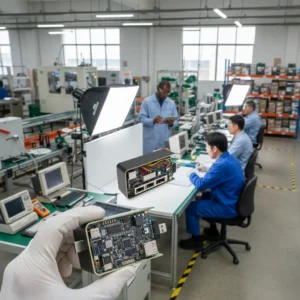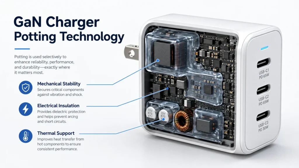
GaN charger potting technology can be difficult for buyers to assess because many suppliers use “potted design” as a shortcut for quality. That claim can create problems when the actual charger has weak thermal design, inconsistent assembly, or incomplete safety documentation. We help buyers look beyond the glue and evaluate the complete product system.
GaN charger potting technology is the use of an insulating compound to secure and encapsulate selected internal components, PCB areas, or assemblies inside a charger1. It can support mechanical stability, vibration resistance, and thermal management2, but it does not automatically make a charger safer, cooler, or more reliable. Buyers should verify the potting material, coverage area, thermal design, finished-product tests, certifications, and batch-quality controls before placing a bulk order.
In our discussions with European and U.S. buyers, we often see the same question: “Is this charger fully potted?” It is a reasonable starting point, but it is not the final question. The better sourcing question is what risk the potting design addresses—and how the supplier proves the complete charger performs consistently.
What Is GaN Charger Potting Technology in a Charger?
Buyers may hear terms such as “full potting,” “glue filling,” or “encapsulation” without receiving a clear explanation. This creates uncertainty, especially when comparing compact GaN charger suppliers with very different prices. A vague claim does not show what is actually inside the product.
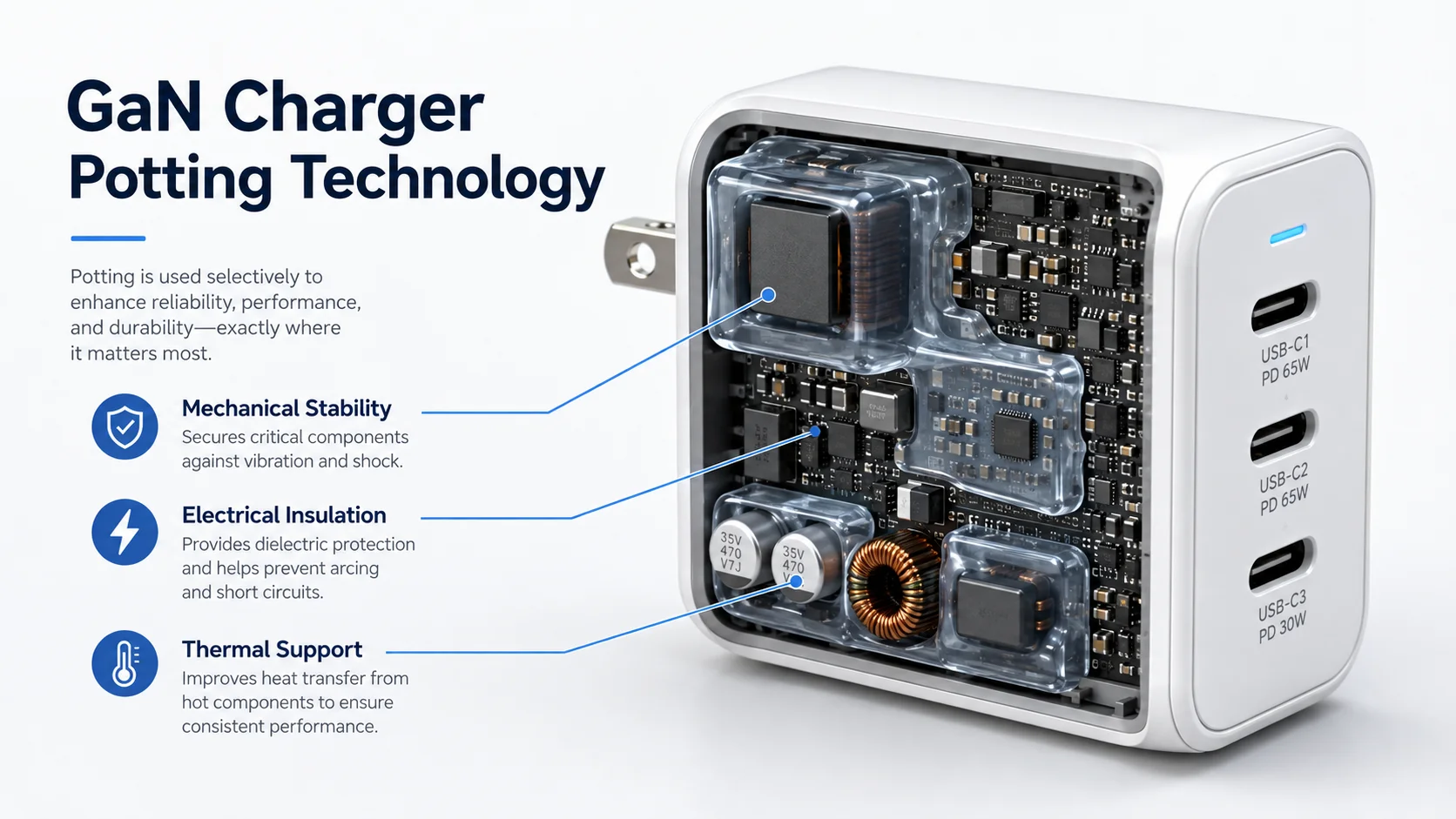
GaN charger potting technology refers to applying a resin, silicone, epoxy, or other encapsulation compound around selected internal electronic areas. The compound may secure components, reduce movement, provide electrical insulation, and support heat transfer depending on the material and design. Coverage can be partial or extensive, and it varies by charger model.
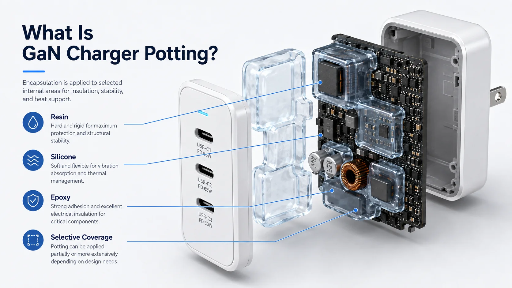
In simple terms, potting is an internal filling process. A supplier dispenses a compound into a defined area of the charger after the PCB assembly reaches a suitable production stage. The material then cures under controlled conditions.
However, buyers should not assume that every area inside a charger is potted. A supplier may use potting around:
- High-voltage components
- Transformers or inductors
- Capacitors and surrounding PCB zones
- AC input sections
- USB-C output areas
- Components that need additional mechanical support
Potting Is a Design Choice, Not a Universal Quality Label
At our Shenzhen-side product discussions, we ask suppliers to explain what is potted, why it is potted, and how the process is controlled. Those three questions often reveal more than a marketing image of a charger filled with black or gray compound.
A potted GaN charger can be well designed. It can also be poorly designed if the supplier uses unsuitable materials, inconsistent dispensing, or weak heat paths. Likewise, some non-potted or partially potted GaN chargers can perform well when they have appropriate component selection, enclosure design, insulation distances, and verified safety performance.
Buyers should request written confirmation covering:
| Information to Request | Why It Matters |
|---|---|
| Potting material category | Helps buyers understand whether the supplier uses silicone, epoxy, or another compound |
| Potting coverage area | Clarifies whether the design is fully or partially encapsulated |
| Intended function | Shows whether potting supports stability, insulation, thermal transfer, or another purpose |
| Process controls | Indicates how the supplier manages dispensing and curing consistency |
| Finished-product checks | Connects the process to real charger performance |
Why Do Compact GaN Chargers Use Potting Technology?
Ultra-compact chargers promise high output power in a small enclosure. That design goal creates challenges because components sit closer together, internal space is limited, and assembly tolerances become more important. Buyers may worry that a small charger cannot manage heat or survive repeated transport.
Compact GaN chargers may use potting technology to stabilize internal components and support the overall mechanical and thermal design. GaN devices can enable smaller charger designs3, but the finished product still needs careful layout, insulation, component spacing, enclosure design, and validation. Potting is only one part of that system.
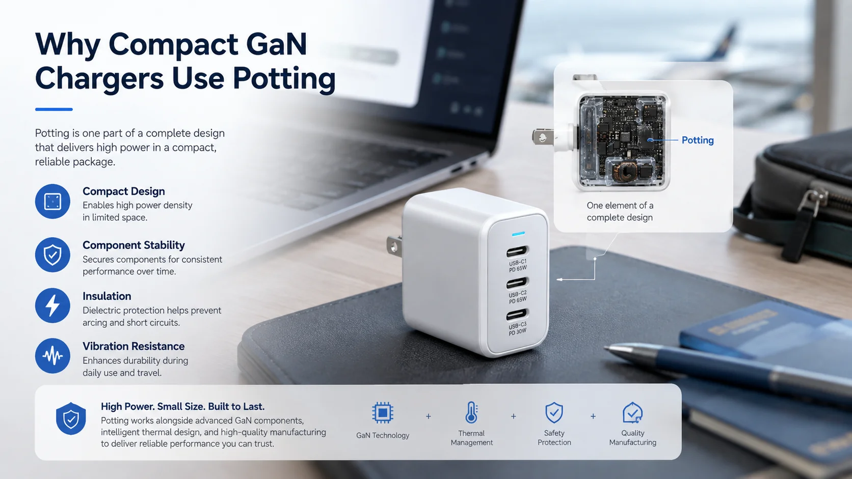
GaN semiconductor technology can support higher switching efficiency and smaller magnetic components compared with many traditional silicon-based charger designs4. This is one reason buyers see 30W, 45W, 65W, and higher-power USB-C chargers in increasingly compact formats.
Still, compactness increases sourcing risk if a factory pushes the design too far without sufficient validation.
Why Space Changes the Manufacturing Discussion
When internal components are close together, movement during shipping, drops, or repeated plug-and-unplug cycles may affect solder joints, leads, or component positioning5. Potting may help reduce some of that movement.
A well-controlled potting approach can potentially support:
- Component stabilization: It can limit movement of selected components.
- Vibration resistance: It may reduce stress caused by transport vibration.
- Assembly consistency: It can help hold parts in place where the design requires it.
- Electrical insulation support: Appropriate compounds may contribute to insulation in defined areas.
- Enclosure fit: It may help support a compact internal layout.
But buyers should avoid treating potting as a substitute for core engineering. The supplier still needs a suitable PCB layout, properly rated components, safe clearances, reliable soldering, and a housing that fits the intended market.
I have seen buyers focus heavily on the external size of a 65W GaN charger sample. The smaller housing often looks more attractive on a retail shelf, but the smarter discussion is whether that small housing has been validated under intended load, ambient temperature, and long-term use conditions. A good supplier should connect its compact design claims to finished-unit evidence.
How Does GaN Charger Potting Technology Affect Heat Dissipation?
Heat is one of the first concerns buyers raise about compact fast chargers. Some buyers believe potting traps heat. Others assume that potting automatically improves cooling. Both assumptions can be misleading because thermal performance depends on the complete charger design6.
GaN charger potting technology can either support or hinder heat management depending on the compound’s thermal properties, coverage location, thickness, and connection to the charger’s heat-transfer path7. Buyers should review temperature-rise evidence for the complete model instead of assuming that more potting always means better cooling.
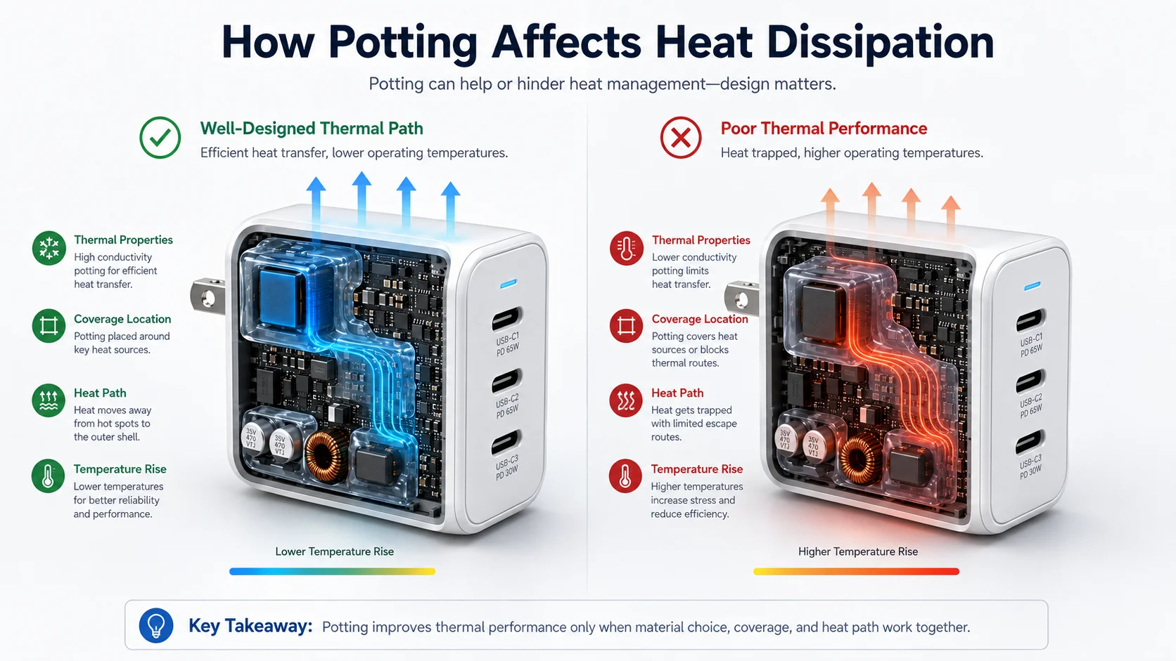
A charger generates heat through several components and conversion stages. The final temperature depends on power level, efficiency, component selection, PCB design, enclosure material, airflow, room temperature, load profile, and the way heat moves away from internal parts.
Thermal Conductivity Is Not the Whole Story
A potting material may be selected partly for its thermal characteristics. Yet material selection alone does not prove the charger will run cooler. A thermally suitable compound needs to be applied in the correct location and integrated into a functional heat path.
Buyers should ask practical questions:
-
Which areas receive potting compound?
The answer should identify the relevant PCB or component zones. -
What is the intended thermal purpose?
The supplier should explain whether the material supports heat transfer, insulation, mechanical stability, or multiple functions. -
What finished-product temperature information is available?
Ask for model-specific testing information under stated conditions. -
What output modes were tested?
A multi-port GaN charger may behave differently when one or more ports operate simultaneously. -
How does the supplier control batch consistency?
Dispensing quantity, placement, and curing conditions can affect process repeatability.
We recommend that buyers compare temperature-related information across the same power class and charger format. A 65W charger should not be evaluated only against a 20W charger, and a single-port model should not be compared casually with a multi-port model.
For market-specific decisions, buyers should also use qualified compliance and product-safety professionals. The supplier’s documentation should support—not replace—independent evaluation where required.
Potted vs Non-Potted GaN Chargers: What Should Buyers Compare?
Many sourcing decisions become too simple: potted equals premium, while non-potted equals low quality. That shortcut can lead buyers to reject viable suppliers or accept weak products with impressive internal photos. The real issue is how the design manages its intended risks.
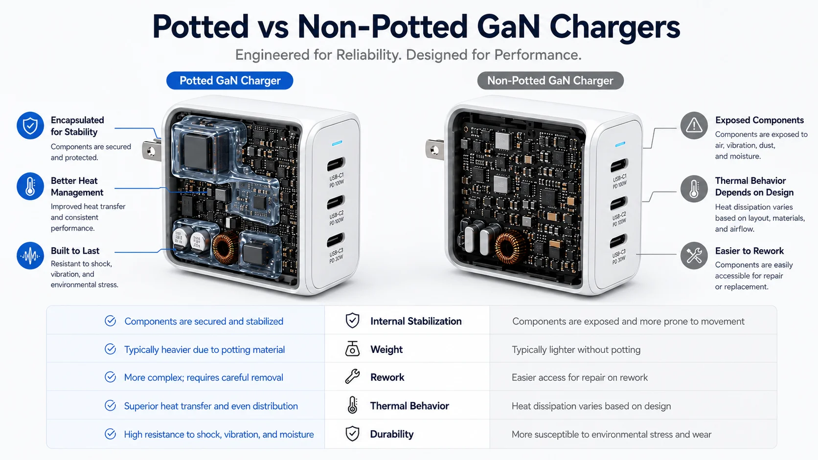
Potted and non-potted GaN chargers can both be suitable when their complete designs are properly validated. Potted designs may offer added internal stabilization, while non-potted designs may offer lower weight and easier rework8. Buyers should compare heat management, safety evidence, durability checks, manufacturing controls, and total channel risk.
| Design Factor | Potted GaN Charger | Non-Potted or Lightly Potted GaN Charger | What Buyers Should Verify |
|---|---|---|---|
| Size potential | Can support dense internal layouts | Can also be compact with good engineering | Internal structure and enclosure dimensions |
| Heat management | Depends on compound and thermal path | Depends on layout, components, and enclosure | Model-specific temperature evidence |
| Drop and shock resistance | May reduce movement in selected areas | Relies more on mechanical design and assembly | Drop, vibration, and post-test function checks |
| Weight | Often may be heavier | Often may be lighter | Actual unit weight and retail requirements |
| Manufacturing complexity | Requires dispensing and curing controls | May involve fewer encapsulation steps | Process consistency and factory controls |
| Repairability | Usually more difficult to rework | Often easier to inspect or repair | Service strategy and defect analysis process |
| Cost | May increase material and process cost | May reduce some direct process cost | Transparent quotation comparison |
| Buyer risk | Lower only if well designed and controlled | Not automatically higher | Whole-unit safety, QC, and after-sales evidence |
This table is useful during supplier comparison, but it should not replace sample evaluation. We suggest buyers compare samples side by side instead of relying only on supplier statements.
Does GaN Charger Potting Technology Improve Drop Resistance?
Retail buyers face real return costs when chargers arrive damaged, fail after transit, or develop intermittent charging issues. A charger may look intact after a drop while internal parts have shifted or solder joints have been stressed. This is why mechanical durability deserves attention before bulk purchasing.
GaN charger potting technology may improve resistance to component movement, vibration, and some mechanical stress by supporting internal parts9. However, it does not guarantee drop resistance because performance also depends on housing strength, PCB mounting, solder quality, component placement, and the supplier’s finished-product validation.
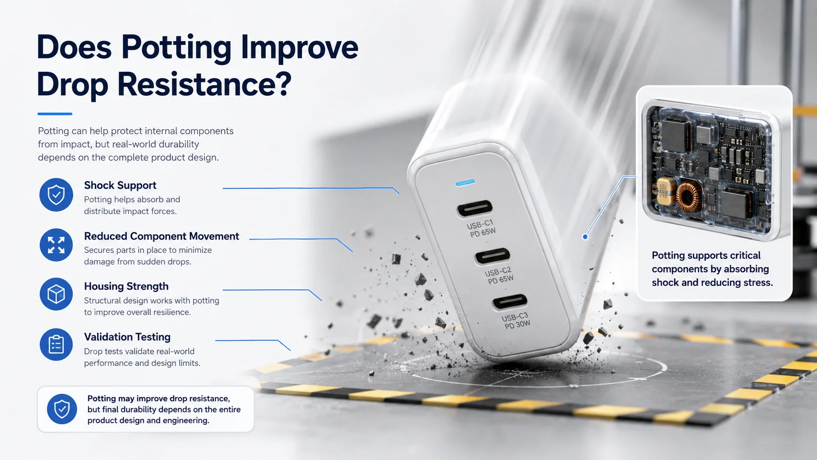
The main potential benefit is stabilization. If selected components are held more securely, they may be less likely to move under vibration or shock. This can be relevant for chargers that travel through long export routes, warehouse handling, retail distribution, and consumer use.
What We Would Check During Sample Review
When we review a GaN charger sample, we do not judge it only by whether the charger still powers on after one basic drop. We look for a more complete approach:
- Does the enclosure show cracks, gaps, or separation?
- Does the USB-C port remain secure and aligned?
- Does the charger maintain stable output after mechanical testing?
- Does the plug assembly remain firmly attached?
- Does the supplier document the test method and acceptance criteria?
- Are samples from the same production process intended for mass production?
A potted assembly can still fail if the housing is weak or the process creates stress around components. Excessive or poorly placed compound can also create its own manufacturing challenges. For this reason, buyers should ask for objective test records where available and include appropriate mechanical checks in their sample approval plan.
Does GaN Charger Potting Technology Make Chargers Heavier or Less Safe?
Some buyers avoid potted chargers because they expect them to be heavy, impossible to repair, or potentially unsafe. These concerns are worth discussing, but broad conclusions are not helpful. The answers depend on the amount and type of compound used.
GaN charger potting technology can add weight and reduce repairability, especially when coverage is extensive. It is not inherently unsafe when suitable materials and processes are used, but buyers should ask the supplier to document the material category, intended application, safety-related evidence, and disposal or handling information where relevant.
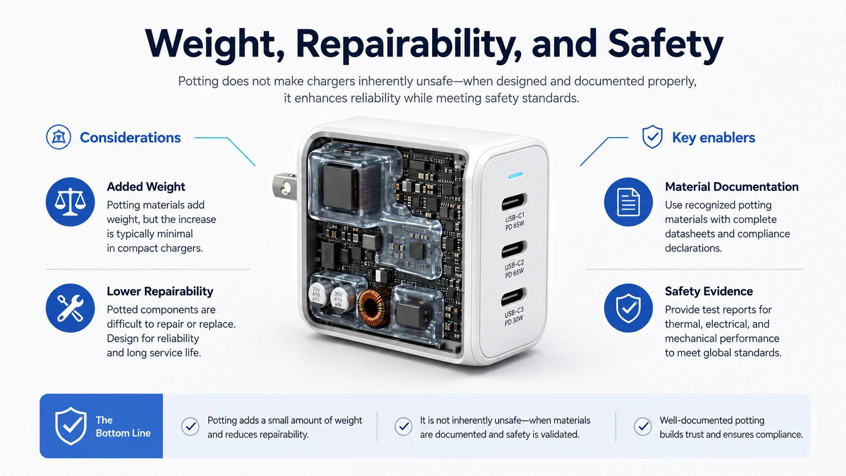
Potting compound adds material to the charger, so it can increase unit weight10. Whether that matters depends on the product category. A compact travel charger sold as an ultra-light accessory may require closer comparison than a desktop multi-port charger.
Repairability is another trade-off. Extensive encapsulation can make internal inspection, rework, and failure analysis more difficult. For branded buyers with warranty programs, this can affect after-sales planning.
Buyers should request:
- Material identification or category information
- Applicable safety and compliance documentation for the charger model
- Information on restricted-substance compliance where required
- A clear explanation of whether the design is partial or fully potted
- A supplier procedure for analyzing returned or failed units
The key point is simple: potting should be documented as part of a controlled production process, not treated as a mystery material inside the housing.
Why Do Some Low-Cost GaN Chargers Reduce Potting?
Price differences between similar-looking GaN chargers can be surprising. Buyers may see two products with similar wattage, ports, and exterior styling, yet one quotation is significantly lower. Potting coverage and process control can be part of the difference, although they are never the only explanation.
Some low-cost GaN charger suppliers may reduce or skip potting to lower material use, labor, curing time, and production complexity11. This does not automatically mean the charger is unacceptable, but buyers should investigate whether the lower price reflects a different reliability strategy, weaker process control, or reduced finished-product validation.
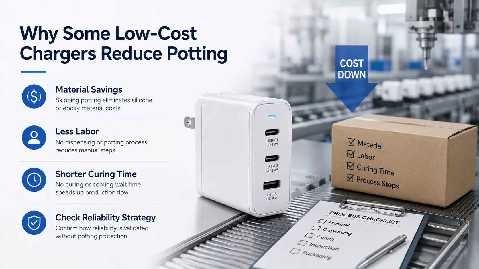
A lower-cost supplier may use:
- No potting compound
- Partial potting only in selected areas
- Lower-cost compound options
- Less tightly controlled dispensing volumes
- Shorter or less controlled curing steps
- A different PCB, transformer, capacitor, or enclosure design
None of these points alone proves poor quality. The issue is whether the supplier can explain the design and provide evidence that the finished charger meets the buyer’s intended quality, safety, and channel requirements.
Avoid Price-Only Comparisons
We recommend comparing quotations using a structured checklist. A lower unit price may become more expensive if it leads to higher return rates, delayed shipments, compliance issues, or retailer complaints.
For retail and chain buyers, the relevant cost is not only the factory price. It is also the potential cost of returns, customer-service workload, replacement stock, and brand reputation.
Ask suppliers to quote against the same specification: output configuration, plug type, housing material, cable inclusion, packaging, certification requirements, MOQ, lead time, and inspection expectations. This makes the comparison more meaningful.
How Should Buyers Verify GaN Charger Potting Technology Before Bulk Ordering?
A supplier can provide attractive product images and say that a charger is “high reliability.” Yet bulk orders involve a different level of risk than sample purchases. Buyers need a verification plan that links internal design claims to finished-product quality and production consistency.
Buyers should verify GaN charger potting technology through written design information, sample comparisons, finished-unit temperature and functional checks, mechanical testing, applicable certification documents, factory process review, and pre-shipment quality control. Potting should be evaluated as one part of the complete GaN charger sourcing process.
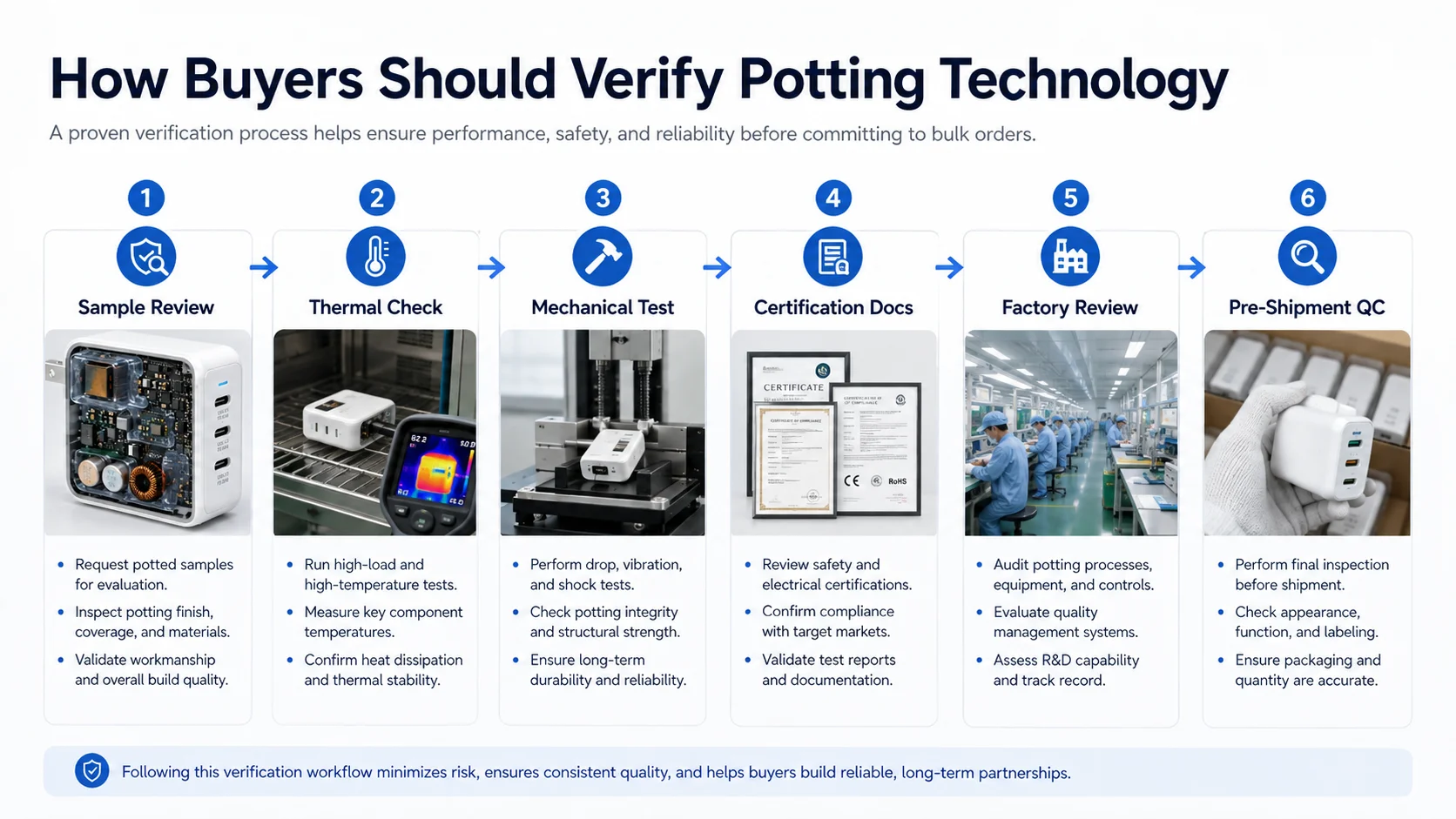
Here is the practical sequence we recommend.
1. Request Clear Internal-Design Information
Ask the supplier to confirm:
- Whether the charger uses partial or extensive potting
- The potting material category
- Which areas are covered
- The intended purpose of the potting
- Any key dispensing and curing controls
Avoid accepting general phrases such as “premium glue” or “full protection” without supporting details.
2. Compare Physical Samples
Request samples from shortlisted GaN charger suppliers. Compare external finish, weight, port alignment, plug construction, charging performance, packaging, and operating behavior. If possible, compare samples at the same power level and port configuration.
3. Review Whole-Unit Evidence First
Potting is not the first screening gate. We recommend buyers first request applicable certifications and safety-related documents for the specific charger model and destination market. Buyers should also ask for available temperature-rise information and relevant functional test records.
Certification claims should always be verified against the applicable documents, model numbers, factories, and target-market requirements12.
4. Include Reliability Checks in Sample Approval
The sample plan may include checks for:
- Output stability under intended loading conditions
- Temperature behavior under stated test conditions
- Drop or shock resistance
- Plug and port mechanical integrity
- Aging or burn-in procedures where appropriate
- Cosmetic finish after testing
5. Verify Mass-Production Controls
A good sample is not enough. Buyers should ask how the supplier controls production consistency. For potting, this may include material storage, dispensing settings, curing requirements, operator instructions, and inspection records.
At KingSourcing, we can help buyers compare GaN charger suppliers, verify samples, review factory processes, arrange inspections, and manage quality checks before bulk production. Our goal is not to claim that one construction method is always superior. Our goal is to reduce avoidable sourcing risk.
Frequently Asked Questions
Is a fully potted GaN charger always better?
No. A fully potted GaN charger may offer more internal stabilization, but it is not automatically safer or more durable. Buyers should assess the complete design, including thermal performance, safety documentation, component selection, housing strength, manufacturing controls, and finished-product test evidence.
Does potting make a GaN charger run hotter?
Potting can affect heat behavior, but it does not always make a charger hotter. The result depends on the material, placement, thickness, thermal path, power level, enclosure design, and other factors. Buyers should request temperature-related evidence for the exact charger model.
What should I ask a GaN charger supplier about potting?
Ask what material category is used, where it is applied, whether coverage is partial or extensive, why it is used, and how the supplier controls dispensing and curing. You should also request model-specific safety, temperature, and quality documentation.
Can a non-potted GaN charger be reliable?
Yes. A non-potted or lightly potted charger can be reliable when the complete design is appropriate and validated. Reliability depends on component quality, PCB layout, insulation, soldering, housing design, thermal management, and consistent production—not potting alone.
Why does potting matter for retail buyers?
Potting may affect mechanical stability, internal consistency, weight, and repairability. For retailers and brand owners, the larger concern is batch-quality risk. Inconsistent execution can contribute to returns, complaints, warranty costs, and damage to customer trust.
Conclusion
GaN charger potting technology is worth reviewing, but it should never be used as a stand-alone measure of charger quality. A responsible buyer evaluates what is potted, why the supplier uses it, how the process is controlled, and how the complete charger is validated. We recommend comparing samples, checking applicable documents, reviewing temperature and reliability evidence, and verifying mass-production controls before confirming a bulk order. Contact KingSourcing to support your GaN charger supplier selection, sample review, factory verification, and pre-shipment QC process.
Related topics: GaN charger potting technology, GaN charger manufacturing, compact GaN chargers, potted GaN charger, GaN charger heat dissipation, GaN charger supplier China, wholesale GaN chargers, China charger sourcing, GaN charger quality control
"Potting (electronics) - Wikipedia", https://en.wikipedia.org/wiki/Potting_(electronics). Electronic potting is the encapsulation of components or assemblies in a polymeric material, commonly used to provide environmental protection, electrical insulation, and mechanical support. Evidence role: definition; source type: education. Supports: Electronic potting and encapsulation involve surrounding electronic components or assemblies with a polymeric compound for protection, insulation, or mechanical support.. ↩
"Comparative Characterization of Electronic Packaging Materials ...", http://etd.auburn.edu/handle/10415/2261. Studies of electronic encapsulation show that potting compounds can alter mechanical support, vibration behavior, electrical insulation, and heat transfer, with the result depending on material properties and assembly geometry. Evidence role: mechanism; source type: paper. Supports: Encapsulation materials can affect mechanical restraint, vibration response, insulation, and heat transfer in electronic assemblies.. Scope note: These effects are design- and material-dependent and do not establish the performance of any individual charger. ↩
"Gallium nitride - Wikipedia", https://en.wikipedia.org/wiki/Gallium_nitride. Gallium-nitride power devices can support high-frequency power conversion, which may permit smaller magnetic and passive components and thereby contribute to more compact converter designs. Evidence role: mechanism; source type: research. Supports: GaN power devices can operate efficiently at higher switching frequencies, which can reduce the size of passive components in power converters.. Scope note: Device-level capability does not by itself determine the size, efficiency, safety, or thermal performance of a finished charger. ↩
"Power Electronics Revolutionized: A Comprehensive Analysis ...", https://pmc.ncbi.nlm.nih.gov/articles/PMC10673564/. Power-electronics literature reports that GaN devices can enable high-frequency and efficient converter operation, often allowing reduced magnetic-component size relative to comparable conventional silicon-based designs. Evidence role: general_support; source type: paper. Supports: Reviews of wide-bandgap power electronics describe GaN devices as capable of high-frequency, high-efficiency operation that can reduce passive-component size relative to conventional silicon implementations.. Scope note: Comparative efficiency and size depend on topology, operating conditions, component selection, and implementation quality. ↩
"[PDF] NASA-DOD LEAD-FREE ELECTRONICS PROJECT", https://ntrs.nasa.gov/api/citations/20100029736/downloads/20100029736.pdf. Electronic-reliability guidance recognizes shock and vibration as sources of mechanical stress that can damage component attachments and contribute to solder-joint fatigue or failure. Evidence role: mechanism; source type: institution. Supports: Shock and vibration can produce mechanical stresses in electronic assemblies that contribute to damage or fatigue in solder interconnects and component attachments.. Scope note: The susceptibility of an individual charger depends on its mechanical design, materials, mounting method, and actual transport or use conditions. ↩
"7.0 Thermal Control - NASA", https://www.nasa.gov/smallsat-institute/sst-soa/thermal-control/. Thermal analysis of electronic equipment treats component dissipation, board layout, thermal interfaces, enclosure properties, airflow, and ambient conditions as interacting determinants of operating temperature. Evidence role: mechanism; source type: research. Supports: Electronic equipment temperature is governed by heat generation and the complete thermal path, including components, board layout, interfaces, enclosure, and surrounding environment.. Scope note: The source provides a general thermal-design framework and does not substitute for model-specific charger temperature testing. ↩
"In situ Thermoreflectance Characterization of Thermal ...", https://pubmed.ncbi.nlm.nih.gov/35573030/. Research on electronic encapsulation and thermal interfaces indicates that an encapsulant's effect on heat removal depends on its conductivity, thickness, interfaces, placement, and the overall thermal path. Evidence role: mechanism; source type: paper. Supports: The thermal effect of an encapsulant depends on thermal conductivity, layer thickness, contact resistance, coverage geometry, and its connection to heat-removal surfaces.. Scope note: A material's nominal thermal conductivity alone cannot predict the temperature rise of a particular charger. ↩
"Epoxy vs. Silicone: Selecting the Optimal Potting Material ...", https://www.allpcb.com/allelectrohub/epoxy-vs-silicone-selecting-the-optimal-potting-material-for-harsh-environment-electronics. Electronics-packaging references describe potting as a means of mechanical and environmental protection, while noting that extensive encapsulation can increase material mass and make inspection, repair, and rework more difficult. Evidence role: general_support; source type: research. Supports: Potting can provide mechanical protection and support, while extensive encapsulation can impede inspection, repair, and rework and adds material mass.. Scope note: The magnitude of these trade-offs varies with compound type, coverage, product architecture, and repair process. ↩
"[PDF] Experimental Study of PCB Vibration Induced by MLCC Assembly ...", https://scholarsmine.mst.edu/cgi/viewcontent.cgi?article=7816&context=ele_comeng_facwork. Experimental and modeling studies of encapsulated electronic assemblies show that potting materials can constrain component motion and modify vibration and shock responses. Evidence role: mechanism; source type: paper. Supports: Encapsulation can mechanically constrain components and alter their response to vibration and shock loading.. Scope note: Encapsulation may also introduce stress through curing, thermal expansion mismatch, or unsuitable geometry; it does not guarantee drop-test performance. ↩
"Low-cost and prototype-friendly method for biocompatible ... - PMC", https://pmc.ncbi.nlm.nih.gov/articles/PMC9887057/. Because encapsulation compounds have material density, applying them to an electronic assembly increases assembly mass by an amount determined by the compound volume and density. Evidence role: general_support; source type: research. Supports: Potting compounds have nonzero density and therefore add mass in proportion to the amount applied.. Scope note: The resulting weight increase can be negligible or substantial depending on coverage and charger size. ↩
"Potting and Encapsulation in Electronics Manufacturing", https://www.practicaltechnologies.us/potting.html. Electronic potting processes typically add material-handling, dispensing, curing, and inspection operations to assembly, so omitting or reducing encapsulation can reduce associated material use and process steps. Evidence role: mechanism; source type: education. Supports: Electronic potting generally requires material preparation, dispensing, cure control, and inspection steps in addition to board assembly.. Scope note: This does not demonstrate why a particular supplier's price is lower or establish that reduced potting reflects inadequate quality control. ↩
"Consumer Product Safety Commission", https://www.cpsc.gov/. Official product-safety guidance requires manufacturers and importers to ensure that electrical products meet applicable conformity requirements and that supporting technical documentation and product identification are available for assessment. Evidence role: expert_consensus; source type: government. Supports: Electrical products placed on regulated markets require conformity assessment and technical documentation applicable to the product and relevant legal requirements.. Scope note: Specific legal duties vary by jurisdiction, product category, sales channel, and the role of the economic operator. ↩